- 您现在的位置:买卖IC网 > Sheet目录362799 > EVAL-AD1937EB (Analog Devices, Inc.) 4 ADC/8 DAC with PLL, 192 kHz, 24 Bit CODEC
Preliminary Technical Data
AD1935/AD1936/AD1937/AD1938/AD1939
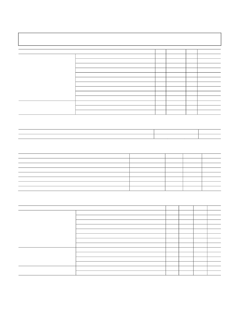
Parameter
Rev. Pr
I
| Page 3 of 30
Min
-0.5
-30
0.90
Typ
-15
-10
100
0
0.375
95
100
1.50
1.50
1.50
Max
+0.5
30
±0.6
1.80
Unit
dB
mV
mV
ppm/°C
dB
Degrees
dB
dB
dB
V
V
V
Interchannel Gain Mismatch
Offset Error, Single-ended version
Offset Error, Differential version
Gain Drift
Interchannel Isolation
Interchannel Phase Deviation
Volume Control Step
Volume Control Range
De-emphasis Gain Error
Output Resistance at Each Pin
Internal Reference Voltage, FILTR
External Reference Voltage, FILTR
Common-Mode Reference Output, CM
REFERENCE
Table 2
Crystal Oscillator
Parameter
Transconductance
Min
Typ
10
Max
Unit
mmhos
Table 3
Digital I/O
Parameter
Input Voltage HI (V
IH
)
Input Voltage LO (V
IL
)
Input Leakage (I
IH
@ V
IH
= 2.4 V)
Input Leakage (I
IL
@ V
IL
= 0.8 V)
High Level Output Voltage (V
OH
) I
OH
= 4 mA
Low Level Output Voltage (V
OL
) I
OL
= 4 mA
Input Capacitance
Min
2.0
DVDD – 0.5
Typ
Max
0.8
10
10
0.5
5
Unit
V
V
μA
μA
V
V
pF
Table 4
Power Supplies
Parameter
Min
3.0
3.0
Typ
3.3
3.3
56
TBD
TBD
74
TBD
TBD
429
185
244
TBD
TBD
TBD
Max
3.6
3.6
Unit
V
V
mA
mA
mA
mA
mA
mA
mW
mW
mW
mW
dB
dB
Voltage, DVDD
Voltage, AVDD
Digital Current
Digital Current—Power-Down
Digital Current—Reset
Analog Current
Analog Current—Power-Down
Analog Current—Reset
Operation—All Supplies
Operation—Digital Supply
Operation—Analog Supply
Power-Down—All Supplies
1 kHz 200 mV p-p Signal at Analog Supply Pins
20 kHz 200 mV p-p Signal at Analog Supply Pins
Supplies
Dissipation
Power Supply Rejection Ratio
Table 5
发布紧急采购,3分钟左右您将得到回复。
相关PDF资料
Eval-AD1940EB
SigmaDSP-TM Multichannel 28-Bit Audio Processor
EVAL-AD1953EB
16-bit fixed point DSP with Flash
EVAL-AD1958EB
PLL/Multibit DAC
EVAL-AD1959EB
PLL/Multibit DAC
EVAL-AD1974EB
4 ADC with PLL, 192 kHz, 24-Bit Codec
EVAl-AD1974EBZ
4 ADC with PLL, 192 kHz, 24-Bit Codec
EVAL-AD1990EB
Audio Switching Amplifier
EVAL-AD1992EB
Audio Switching Amplifier
相关代理商/技术参数
EVAL-AD1937EBZ
制造商:Analog Devices 功能描述:EB SINGLE CHIP CODEC 4 ADC'S W/DIFF OUTP - Boxed Product (Development Kits)
EVAL-AD1938AZ
功能描述:BOARD EVAL FOR AD1938 RoHS:是 类别:编程器,开发系统 >> 评估演示板和套件 系列:- 标准包装:1 系列:PSoC® 主要目的:电源管理,热管理 嵌入式:- 已用 IC / 零件:- 主要属性:- 次要属性:- 已供物品:板,CD,电源
EVAL-AD1938EB
制造商:AD 制造商全称:Analog Devices 功能描述:4 ADC/8 DAC with PLL, 192 kHz, 24-Bit CODEC
EVAL-AD1938EBZ
制造商:Analog Devices 功能描述:EVAL BD FOR MULTI CHANNEL 96KHZ CODEC - Boxed Product (Development Kits)
EVAL-AD1939AZ
功能描述:BOARD EVAL FOR AD1939 RoHS:是 类别:编程器,开发系统 >> 评估演示板和套件 系列:- 标准包装:1 系列:PCI Express® (PCIe) 主要目的:接口,收发器,PCI Express 嵌入式:- 已用 IC / 零件:DS80PCI800 主要属性:- 次要属性:- 已供物品:板
EVAL-AD1939EB
制造商:Analog Devices 功能描述:EVAL - Bulk
EVAL-AD1940AZ
功能描述:BOARD EVAL AD1940 SIGMADSP RoHS:是 类别:编程器,开发系统 >> 评估演示板和套件 系列:SigmaDSP® 标准包装:1 系列:PCI Express® (PCIe) 主要目的:接口,收发器,PCI Express 嵌入式:- 已用 IC / 零件:DS80PCI800 主要属性:- 次要属性:- 已供物品:板
EVAL-AD1940EB
制造商:Analog Devices 功能描述:DEV TOOLS, SIGMADSPTM MULTICH 28BIT AUD PROCESSOR - Bulk